
|
||||
|
|
||||
|
|
||||
|
||||
|
|
PROJECT SUMMARY
A manifestation of the human tendency to generate comfortable environments, it is evidenced in their desire to replace the basic necessity of communication. To have the possibility to consent to the information in any place, condition and time has impelled the demand of portable systems. As answer to this growing demand, the academy and the electronic industry have developed wireless systems of transmission and reception (transceivers) which have acquired great importance in the world technological scenario.
This project proposes the design and implementation of a integrated transceiver in CMOS technology of very low power consumption, to be used in applications of short reach fulfilling the minimum specifications of the Bluetooth standard. The circuit integrated resultant will motivate the formation process and study of the microelectronic by means of the orientation of the work carried out in the classrooms, toward the electronic design thinking on integrated systems; in this way the resided problems in the acepted conception of discrete electronic at local level is being solved, this conceptions lacks of competitiveness in the world enviroment, having the possibility that these integrated systems are implemented, according to the options of production at academic level without any cost or at very low costs [1, 2].
The above, will establish a technological precedent which demonstrates to the national industry that the academy is a real option for the design of integrated circuits, making viable future investments in this area. Additionally, it will be reinforced presenting publications to the international academic community, indicating that the Colombian academy is interested in the study and development of new technologies.
[1] Circuits Multi-Projects, CMP Std., 2004. [Internet]. Visite: http://cmp.imag.fr/
[2] Integrated Circuit Prototype Fabrication and Low Volume Production, MOSIS Service, MOSIS Std.,
2004. [Internet]. Visite: http://www.mosis.org/PROBLEM DESCRIPTION
Initially, the industry developed radiofrecuency circuits in technologies of good performance at high frequencies (Bipolar, GaAs, BiCMOS). Nevertheless, the high costs of those technologies and the integration Incompatibility with the digital processing system, which are commonly carried out in technology CMOS, compromise the decrease of costs and size of the wireless systems.
A transceiver is constituted by a radiofrequency system (RF) and a digital processing system. The continuos decrease of the transistor's dimensions in CMOS technologies, which has allowed bigger integration and better perfomance of the digital circuit, and the increase of the working frequency have profiled the CMOS technology as an option aviable to the implementation of RF circuits.
Currently Colombia doesn't have the developed technology necessary for the production of integrated circuits. The systems and electronic equipments used in the country are almost all of them imported from countries where this branch of the productive sector has reached a high development level. The figures for concept of these imports ascend approximately to 36% of the total of the imports made in the last three years. The high costs of these systems are represented so much in their commercial value as in the payments for import taxes that include transport and other commercial tariffs.The above mentioned has led that the acquisition of systems which in other countries are very accessible, would be of difficult obtention for normal people in our country. The big companies overturned their investigations toward the development of devices of better perfomance, smaller power consumption, smaller size and more economic. However due to the commercial pressures, spaces were not presented for the constant development of new devices, therefore the technologies of the time almost stayed wihtout change. On the other hand the universities, free of interests and monetary pressures, began an experimentation stage with technologies until that moment little studied, giving new discoveries as a result in the fields of CMOS technology. The wireless system of transmission and reception inside oneself device (integrated transceiver,) has become a study focus at the present time. This device is in charge of the transmition and reception of signals, therefore, this is one of the
most important elements inside a wireless communication system.In summary, this project propose the design and implementation of a integrated transceiver in CMOS technology with low power consumption, to be used in applications of short reach.
RECEIVER ARCHITECTURE
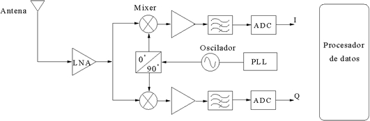
The superheterodine architecture has been broadly used as architecture for wireless receivers. But since the development of portable systems aims to the decrease of the factor size, cost and power, the architecture of direct conversion began to be interesting for the implementation of the receiver.
Receivers with direct conversion also called homodine architecture or zero-IF (Intermediate Frequency similar to zero) are integrated in a single chip due to the selective filters working in middle frequencies are not necessary, generally this filters have to be implemented outside of the chip. However, this architecture maintains disadvantages like the high sensibility to the offset voltage, infiltrations of the local oscillator, mismatches between the route of the direct signal (I) and the route of the signal in quadrature (Q), as well as the distortion of even order and flicker noise that contaminate the band base signal of zero frequency[4].
An alternative to the architecture of direct conversion is the conversion architecture with frequency Intermediate (FI) near to zero, also call of low FI. This architecture is similar to the architecture of direct conversion, in which the RF signal is taken to base band in a single step. However, the wanted signnal is not exactly a base band signal and then the DC values due to infiltrations of the local oscillator, the distortion of even order and the flicker noise don't contaminate the signal. In the same way that in the direct conversion, the problem of the image frequencies stay like in the case of the superheterodine architecture. Because the frequency of the signal taken down to a FI nea to zero should be high to diminish the effects of the noise flicker, the analog-digital conversor (A/D) requires to fulfill the specifications of speed according to the value of the selected FI.
[4] B. Razavi, RF Microelectronics. McGraw-Hill, 1998, ch. 2.
Low Noise Amplifier and Mixer
The problem of design of the low noise amplifier (LNA) and the signal mixer (Mixer) in technology CMOS, tries to be approach in this work by the adaptation of methodologies of design available in state of art, fulfilling the commitments between each of the variables of design for a Bluetooth application at 2.45GHz with an architecture of direct conversion.
Voltage Controlled Oscillator
Voltage Controlled Oscillators (VCO) play an important role at up-conversion and down-conversion processes in wireless communications systems. In order to carry out the latter function, within the required quality conditions, integrated VCO design must negociates trade--offs for to achieve the purposed specifications, on such a way that they converge towards decrease of power consumption, just like mitigate of phase noise and signal distortion. It will adapt a VCO design methodology that approach the former conditions, within requirements of central frequency and phase noise for a Bluetooth IEEE 802.11b system.
TRANSMITTER ARCHITECTURE The transmitter with architecture of direct conversion, requires few omponents in comparison with other architectures. The components required for the architecture of direct conversion are easily integrables, that makes this an interesting architecture in the implementation of the transmitter in an integrated circuit (on-chip). Among the disadvantages of the direct conversion stand out, the signal infiltration of the local oscillator toward the RF signal, the infiltration of the great RF signal toward the mixer and the oscillator taking it to a possible unbalance. Among the blocks that conform the transmitter but that are not yet mentioned in this theoretical mark , they are the digital-analogical
conversor and the power amplifier.
Conversor Digital - Analógico
This project raises the design of a DAC, to be used within the stage of transmission of transceiver integrated in CMOS technology . The designed device must fulfill the requirements of bandwidth, resolution, dynamic range, INL and DNL error, in agreement with the specifications of transceiver, trying to obtain a high performance. Additionally is due to treat to occupy the smaller area possible and to have a low dissipation of power, like requirements of the potabilidad of the system.
| Grupo
en Investigación y Diseño de Circuitos Integrados
- CIDIC |
| Escuela
de Ingenierías Eléctrica, Electrónica y Telecomunicaciones |
| Universidad
Industrial de Santander, Calle 9 Carrera 27 |
| Bucaramanga,
Colombia. |